

 1 day ago
12
PROTECT YOUR DNA WITH QUANTUM TECHNOLOGY
Orgo-Life the new way to the future Advertising by AdpathwayResearchers led by Professor Shulin Sun from Fudan University and Professor Junsuk Rho from Pohang University of Science and Technology have demonstrated high-aspect-ratio all-silicon metasurface devices that achieve broadband, high-efficiency manipulation of terahertz waves. Terahertz radiation, spanning frequencies from 0.1 to 10 terahertz, combines the operational benefits of photonics and electronics for high-speed wireless communications, security inspection, medical diagnosis, and nondestructive imaging. However, conventional terahertz control elements have historically remained hindered by bulky volumes, narrow operational bandwidths, and substantial transmission losses. While all-dielectric metasurfaces can control electromagnetic wavefronts at subwavelength scales, deep etching procedures commonly introduce performance-limiting physical defects such as sidewall tilting, structural depth errors, and lateral dimensional discrepancies.
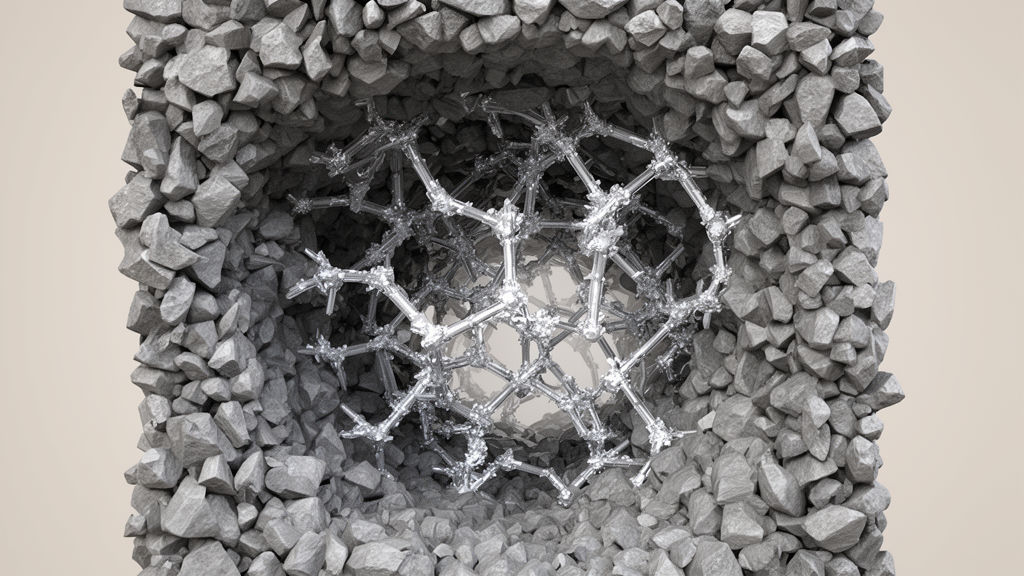
To overcome these microfabrication bottlenecks, the collaborative research team systematically evaluated the influence of etching depth deviation and lateral morphological distortion occurring during the Bosch deep reactive-ion etching process. Through detailed numerical analysis and experimental characterization, the investigators established a dedicated error compensation mechanism. By finely adjusting the cyclical etching and passivation operational parameters, the researchers produced high-aspect-ratio silicon meta-atoms exhibiting strictly vertical sidewalls and precise structural dimensions. The resulting microstructures demonstrated high fabrication repeatability and reached a maximum aspect ratio of 19.2 to 1.
The fabrication framework also solved secondary process deviations that undermine meta-device yield and fidelity. To counter pattern shrinkage caused by high-temperature photoresist baking, the team implemented pre-compensated dimensional offsets directly into the layout design phase, substantially improving process stability. Furthermore, addressing the substantial intrinsic reflection loss caused by the high refractive index of bulk silicon, the engineers integrated specialized antireflective silicon microstructures into the bottom surfaces of the devices. By carefully tailoring the thickness and width of these antireflective features, reflection was minimized, markedly elevating device transmission efficiency while maintaining a broad phase modulation range.
Using this integrated design and manufacturing strategy, the team built and experimentally tested multiple metasurface polarization controllers, including half-wave and quarter-wave plates. The fabricated metasurface half-wave plate demonstrated stable operation across a frequency window of 0.6 to 0.8 terahertz, corresponding to a relative bandwidth of 28.57 percent, while recording a peak polarization conversion efficiency of 0.915 at 0.73 terahertz. Meanwhile, the metasurface quarter-wave plate functioned across a 0.5 to 0.8 terahertz span, delivering a relative bandwidth of 46.15 percent and achieving a peak polarization conversion efficiency approaching 0.99 at 0.66 terahertz. Across all tests, experimental measurements closely matched full-wave electromagnetic simulation profiles.
Extending their methodology from polarization control to complete wavefront shaping, the researchers applied the Pancharatnam–Berry geometric phase concept to fabricate an ultra-efficient terahertz metalens. The resulting focusing device featured an aperture footprint of 10 by 10 square millimeters and an operating numerical aperture of 0.8. Characterization within the 0.6 to 0.8 terahertz operating band revealed an average focusing efficiency of 85.56 percent, calculated as the ratio between the integrated power carried by the cross-polarized focal beam and that of the transmitted terahertz radiation. The experimental focal characteristics aligned with theoretical models and full-wave numerical simulations.
The successful realization of meta-wave-plates and metalenses confirms the viability of systematic Bosch process error compensation for scalable silicon diffractive optics. By providing low loss, broadband operation, high working efficiency, and high fabrication reproducibility, the platform establishes practical foundations for advancing silicon metasurfaces from laboratory proof-of-concept demonstrations into practical engineering systems. The researchers anticipate that these high-aspect-ratio all-silicon metadevices will serve as core functional components in emerging sixth-generation wireless networks, integrated biomedical sensing arrays, and non-destructive industrial inspection systems.
Optical performance evaluations for both the fabricated half-wave plate and quarter-wave plate systematically characterized transmittance efficiency, transmittance phase difference, and the polarization conversion ratio over the operational frequency bands. The experimental measurements matched full-wave numerical simulations across all evaluated parameters, confirming that the microfabricated meta-atoms deliver reliable phase modulation and polarization conversion without suffering from the severe morphological distortions that commonly degrade deep-etched silicon structures. This consistent agreement between experimental data and simulation models validated the efficacy of the error compensation mechanism in preserving precise subwavelength geometries.
The researchers noted that this design and fabrication framework is not restricted to wave-plates and metalenses, but can be extended to the realization of diverse optical metadevices for terahertz wavefront control. Historically, achieving high-efficiency, broadband, and high-fidelity terahertz manipulation at the subwavelength scale has been impeded by conventional deep etching challenges, where sidewall tilting, dimensional deviations, and etching depth errors restrict device quality. By overcoming these microfabrication bottlenecks, the team demonstrated a practical methodology for producing high-aspect-ratio silicon structures that combine low reflection loss, wide bandwidth, and high operational efficiency.
Published in Light: Advanced Manufacturing, the study advances high-precision fabrication technology for high-yield deep silicon etching. By enabling customizable polarization and wavefront manipulation, these high-aspect-ratio silicon metasurface devices provide critical hardware solutions for emerging terahertz applications, including secure communications, high-resolution imaging, non-destructive inspection, and biomedical sensing.
Subject of Research: Deep-etched all-silicon metasurface devices for high-efficiency terahertz manipulation
Article Title: High-aspect-ratio all-silicon metasurface devices for broadband and high-efficiency terahertz wave manipulation
Article References: High-aspect-ratio all-silicon metasurface devices for broadband and high-efficiency terahertz wave manipulation. Original publication (Bibliographic details unavailable.)
Image Credits: AI Generated
DOI: Not provided
Keywords: terahertz waves, all-silicon metasurfaces, deep silicon etching, Bosch process, half-wave plate, quarter-wave plate, metalens, high-aspect-ratio, polarization conversion, focusing efficiency, Pancharatnam-Berry phase, antireflective microstructures, subwavelength optics, Fudan University, POSTECH, terahertz imaging, wavefront manipulation
















 English (US) ·
 French (CA) ·